Integrated Circuits (ICs) are the backbone of modern computing, enabling complex functionalities within compact devices. Their construction involves a sophisticated interplay of materials, each selected for specific electrical, thermal, and structural properties. This article explores the materials used in IC chips, their roles, and their evolution over time.
1. Semiconductor Substrate: Silicon
Primary Material: Silicon (Si)
Role: Serves as the foundational substrate for most ICs due to its excellent semiconductor properties. Silicon’s ability to act as both an insulator and conductor (via doping) makes it ideal for creating transistors.
Why Silicon?
Abundant in nature (from silica sand).
Forms a stable oxide (SiO₂), crucial for insulation and gate dielectrics.
Bandgap (1.1 eV) allows controlled electron flow at room temperature.
Alternative Substrates:
Gallium Arsenide (GaAs): Used in high-frequency applications (e.g., RF chips) due to superior electron mobility.
Silicon-Germanium (SiGe): Combines silicon’s cost-effectiveness with enhanced performance for mixed-signal circuits.
Silicon-on-Insulator (SOI): Adds a buried oxide layer to reduce leakage and improve power efficiency.
2. Doping Elements: Creating Transistors
Materials: Boron (B), Phosphorus (P), Arsenic (As), Antimony (Sb)
Role: Introduced into silicon to create p-type (electron-deficient) and n-type (electron-rich) regions, forming transistors and diodes.
P-type Doping: Boron introduces “holes” (positive charge carriers).
N-type Doping: Phosphorus or arsenic donates free electrons.
Advanced Techniques:
Ion implantation ensures precise dopant distribution.
Annealing repairs silicon lattice damage post-doping.
3. Dielectric Materials: Insulation and Capacitance
Materials:
Silicon Dioxide (SiO₂): Traditional gate dielectric and interlayer insulator.
High-κ Dielectrics (e.g., Hafnium Oxide, HfO₂): Replaced SiO₂ at sub-45nm nodes to reduce leakage currents.
Role:
Isolate conductive layers.
Form capacitor structures in memory cells (e.g., DRAM).
High-κ materials enable thinner layers without compromising insulation.
4. Conductive Materials: Interconnects and Contacts
Materials:
Aluminum (Al): Dominated early ICs for wiring due to ease of etching.
Copper (Cu): Introduced post-1997 (IBM’s Damascene process) for lower resistivity and better electromigration resistance.
Tungsten (W): Used in contacts and vias for high melting point and stability.
Silicides (e.g., Titanium Silicide, TiSi₂): Reduce contact resistance in transistor gates/source-drain regions.
Barrier Layers (e.g., Tantalum Nitride, TaN): Prevent copper diffusion into silicon.
Structure:
Interconnects form a multi-layered “stack” (up to 15 layers in advanced nodes).
Through-Silicon Vias (TSVs) in 3D ICs use copper for vertical connectivity.
5. Packaging Materials: Protection and Connectivity
Materials:
Epoxy Mold Compound: Encapsulates the die, providing mechanical and environmental protection.
Lead Frame/Substrate: Copper or alloy bases for die attachment and pin connections.
Wire Bonds: Gold (Au) or copper wires link the die to the package.
Solder Bumps: Lead-free alloys (e.g., Sn-Ag-Cu) in flip-chip designs for direct mounting.
Heat Spreaders: Copper or aluminum nitride lids dissipate heat.
Thermal Interface Materials (TIMs): Paste/pads (e.g., silicone-based) enhance heat transfer to heatsinks.
6. Advanced and Emerging Materials
Metal Gates: Replaced polysilicon gates (post-45nm) with materials like titanium nitride (TiN) to complement high-κ dielectrics.
2D Materials (e.g., Graphene, MoS₂): Experimental for ultra-thin transistors, though not yet mainstream.
Low-κ Dielectrics (e.g., Porous SiO₂): Reduce capacitive delays in interconnects.
Chalcogenide Alloys: Phase-change materials for non-volatile memory (e.g., Intel’s Optane).
Conclusion
IC chips are marvels of material engineering, combining silicon’s versatility with precise doping, advanced dielectrics, and high-conductivity metals. From the silicon substrate to copper interconnects and protective packaging, each material is optimized for performance, reliability, and scalability. As transistor sizes shrink toward atomic limits, innovations like 2D materials and 3D integration will drive future advancements, ensuring Moore’s Law endures in spirit, if not in literal form.

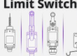
- Everything You Need To Know About Limit Switch - May 21, 2025
- Everthing You Should Know About Rheostat - May 20, 2025
- Everything You Need To Know About Reversing Contactor - May 19, 2025