Semiconductor packaging is a critical yet often overlooked facet of modern electronics, providing protection, power delivery, and signal connectivity to integrated circuits (ICs). As Moore’s Law slows, advanced packaging technologies have emerged as a pivotal enabler of performance gains, offering innovative solutions beyond traditional transistor scaling. This article explores the evolution, key technologies, materials, applications, challenges, and future trends in advanced semiconductor packaging.
2. Evolution of Semiconductor Packaging
Traditional Packaging: Early methods like Dual In-line Package (DIP) and Quad Flat Package (QFP) focused on simplicity and cost-effectiveness. Ball Grid Array (BGA) later improved pin density and thermal performance.
Limitations: Increasing demand for miniaturization, higher speed, and lower power consumption exposed the shortcomings of traditional methods, such as limited I/O density and signal delays.
3. Key Advanced Packaging Technologies
2.5D and 3D IC Packaging:
2.5D: Utilizes silicon or organic interposers to laterally connect dies, enabling high-bandwidth communication (e.g., TSMC’s CoWoS for AI/GPUs).
3D: Stacks dies vertically using Through-Silicon Vias (TSVs), reducing interconnect length and power consumption (e.g., Intel’s Foveros).
Fan-Out Wafer-Level Packaging (FOWLP): Expands I/O density by redistributing connections around the die, widely used in mobile processors (e.g., Apple’s A-series chips).
System-in-Package (SiP): Integrates multiple dies (logic, memory, RF) into a single package, ideal for wearables and IoT devices.
Chiplets and Heterogeneous Integration: Modular dies (“chiplets”) from different process nodes are combined, exemplified by AMD’s EPYC processors, reducing cost and improving yield.
4. Materials and Manufacturing Innovations
Substrates: High-density organic substrates and silicon interposers with low-k dielectrics enhance signal integrity.
Thermal Management: Advanced Thermal Interface Materials (TIMs) and liquid cooling address heat dissipation in 3D stacks.
Interconnects: Microbumps (10–25 µm) and hybrid bonding replace solder balls, enabling finer pitch connections.
5. Applications Driving Demand
High-Performance Computing (HPC): 3D packaging for GPUs/CPUs in data centers.
AI/ML: 2.5D integration of logic and High-Bandwidth Memory (HBM).
5G/IoT : FOWLP and SiP for compact, low-power RF modules.
Automotive: SiP solutions for LiDAR and autonomous driving systems.
Medical Devices: Miniaturized implants using biocompatible packaging.
6. Challenges in Advanced Packaging
Thermal Management: Heat dissipation in densely packed designs.
Signal/Power Integrity: Crosstalk and resistive losses at higher frequencies.
Testing Complexity: Ensuring yield with multi-die systems requires Design-for-Test (DfT) strategies.
Cost and Standardization: High R&D expenses and fragmented ecosystems (e.g., competing chiplet standards).
7. Future Trends and Innovations
Chiplet Ecosystems: Universal standards like UCIe (Universal Chiplet Interconnect Express) to foster interoperability.
Integrated Photonics: Optical interconnects within packages for ultra-low-latency communication.
Sustainability: Recyclable substrates and lead-free materials to meet environmental regulations.
AI-Driven Design: Machine learning tools to optimize package layout and thermal performance.
Conclusion
Advanced semiconductor packaging is no longer a back-end process but a strategic differentiator in the tech industry. By enabling heterogeneous integration, improving power efficiency, and extending Moore’s Law, these technologies are critical for next-gen applications in AI, automotive, and beyond. As the industry embraces chiplets, photonics, and sustainable practices, collaboration across design, manufacturing, and standardization bodies will be key to unlocking their full potential.
Industry Leaders:
TSMC: CoWoS and InFO platforms.
Intel: Foveros 3D and EMIB (Embedded Multi-Die Interconnect Bridge).
Samsung: X-Cube 3D packaging.
ASE Group: SiP solutions for IoT.
This comprehensive approach to advanced packaging ensures continued innovation, bridging the gap between semiconductor capabilities and the escalating demands of modern electronics.

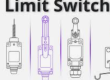
- Everything You Need To Know About Limit Switch - May 21, 2025
- Everthing You Should Know About Rheostat - May 20, 2025
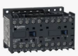
- Everything You Need To Know About Reversing Contactor - May 19, 2025