Dynamic Random-Access Memory (DRAM) is a cornerstone of modern computing, serving as the primary volatile memory in devices from smartphones to supercomputers. This guide delves into the intricacies of DRAM technology, exploring its architecture, types, manufacturing, applications, challenges, and future trends.
Table of Contents
Toggle1. Basics of DRAM
What is DRAM?
DRAM stores each bit of data in a separate capacitor within an integrated circuit. Capacitors charge (1) or discharge (0) to represent binary data. Unlike SRAM (Static RAM), DRAM requires periodic refreshing (every ~64 milliseconds) due to charge leakage.
Key Characteristics
- Volatility: Loses data without power.
- High Density: More cells per area than SRAM, making it cost-effective for main memory.
- Slower Access: Longer latency due to refresh cycles and destructive read operations.
DRAM vs. SRAM
- DRAM: 1 transistor + 1 capacitor per cell; cheaper, higher density, used in main memory.
- SRAM: 6 transistors per cell; faster, no refresh needed, used in CPU caches.
2. Architecture and Operation
Cell Structure (1T1C)
- Transistor: Acts as a switch for data access.
- Capacitor: Stores charge; size impacts retention time and reliability.
Memory Array
- Rows and Columns: Accessed via row/column decoders. Activating a row (page) loads it into a row buffer for column access.
- Banks and Ranks: Banks allow parallel operations; ranks are sets of chips accessed together.
Timing Parameters
- CAS Latency (CL): Delay between column address and data output.
- RAS-to-CAS Delay (tRCD): Time to switch from row to column access.
- Precharge Time (tRP): Time to close a row and open a new one.
3. Types of DRAM
Evolution and Variants
- SDRAM: Synchronous with the system clock (e.g., PC100, PC133).
- DDR SDRAM: Transfers data on both clock edges (DDR1 to DDR5). DDR5 (2020) offers up to 6400 MT/s and 1.1V operation.
- LPDDR: Low-power variants for mobiles (LPDDR5: 5500 MT/s, 0.5V).
- GDDR: High-bandwidth for GPUs (GDDR6X: 21 Gb/s).
- HBM: Stacked dies with TSVs for AI/GPUs (HBM3: 6.4 Gb/s per pin).
Legacy Types
- FPM DRAM: Early PC memory.
- EDO DRAM: Improved FPM with pipelining.
4. Manufacturing Process
Fabrication Steps
- Wafer Production: Silicon wafers prepared via photolithography.
- Capacitor Formation: Trench (embedded) or stacked capacitors for density.
- Testing/Binning: Chips sorted by speed/power; defective cells replaced via redundancy.
- Packaging: DIMMs (desktops), SO-DIMMs (laptops), or BGA (mobile).
Challenges
- Capacitor Scaling: Maintaining capacitance as cells shrink.
- Yield Management: Defect mitigation through redundancy.
5. Applications
- Computing: Main memory in PCs/servers (DDR4/5), caches (HBM).
- Mobile: LPDDR4/5 in smartphones/tablets.
- Graphics: GDDR6/6X in GPUs (NVIDIA RTX 4090).
- Automotive: Robust DRAM for infotainment/ADAS.
- Networking: Buffering in routers/switches.
6. Challenges
- Power Consumption: Refresh cycles drain energy; critical for mobile.
- Scaling Limits: Sub-20nm nodes challenge capacitor reliability.
- Heat Dissipation: High-density modules require cooling.
- Security: Rowhammer attacks mitigated by TRR.
7. Future Trends
- HBM Evolution: More stacks (12+ layers) and higher bandwidth.
- DDR5 Adoption: Mainstream in data centers/PCs.
- 3D DRAM: Vertical cell stacking for density.
- Emerging Tech: MRAM/RRAM for non-volatility; CXL for memory pooling.
- AI-Driven Demand: Faster memories for machine learning workloads.
8. Conclusion
DRAM remains vital despite challenges, evolving to meet demands for speed, density, and efficiency. Innovations like DDR5, HBM3, and 3D architectures ensure its relevance in AI, IoT, and beyond. As JEDEC standards advance, DRAM will continue underpinning the digital world.
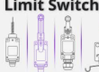
- Everything You Need To Know About Limit Switch - May 21, 2025
- Everthing You Should Know About Rheostat - May 20, 2025
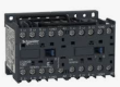
- Everything You Need To Know About Reversing Contactor - May 19, 2025