Integrated Circuit (IC) substrates are critical components in modern electronics, serving as the foundational layer that connects semiconductor chips to printed circuit boards (PCBs). They ensure electrical connectivity, thermal management, and mechanical support, enabling the functionality of devices from smartphones to advanced medical equipment. This article explores the intricacies of IC substrates, including their types, materials, manufacturing processes, applications, and future trends.
1. Definition and Purpose of IC Substrates
An IC substrate is a specialized PCB that acts as an intermediary between a semiconductor die and the main PCB. Its primary functions include:
Electrical Interconnection: Transmitting signals and power between the chip and the PCB through intricate wiring.
Thermal Management: Dissipating heat generated by the chip to prevent overheating.
Mechanical Support: Providing structural stability to protect delicate circuits.
Signal Integrity: Maintaining high-speed signal transmission with minimal loss.
2. Types of IC Substrates
IC substrates are categorized by material and packaging technology:
By Material:
Organic Substrates: Made from epoxy resins (e.g., FR-4, BT resin), these are cost-effective and widely used in consumer electronics.
Ceramic Substrates: Composed of alumina or aluminum nitride, they excel in high-temperature and high-frequency applications (e.g., aerospace, automotive).
Silicon Substrates: Used in advanced 3D packaging (e.g., through-silicon vias, interposers) for high-density interconnects.
By Packaging Technology:
Ball Grid Array (BGA): Uses solder balls for dense connections.
Chip-Scale Package (CSP): Compact design matching the chip size.
Flip-Chip: Directly attaches the die face-down to the substrate for shorter electrical paths.
Wafer-Level Packaging (WLP): Builds substrates directly on the wafer for miniaturization.
3. Materials and Key Properties
Material selection impacts performance:
Thermal Conductivity: Ceramics (24–170 W/mK) outperform organics (0.2–0.5 W/mK).
Coefficient of Thermal Expansion (CTE): Must match silicon (2.6 ppm/°C) to prevent stress during temperature changes.
Dielectric Constant (Dk): Lower Dk (e.g., polyimide: 3.5) enhances high-frequency signal integrity.
Mechanical Stability: Ceramics offer rigidity, while organics provide flexibility.
4. Manufacturing Processes
Key steps include:
Subtractive Process: Etching copper-clad laminates to form circuits.
Semi-Additive Process (SAP): Electroplating fine traces for high-density interconnects (HDI).
Laser Drilling: Creating microvias (<150 µm) for layer connections.
Build-Up Layers: Adding dielectric and conductive layers to increase density.
Surface Finishing: Applying solder mask and finishes like ENIG (Electroless Nickel Immersion Gold).
5. Advanced Technologies
High-Density Interconnect (HDI): Enables finer lines/spaces (≤40 µm) for miniaturization.
Through-Silicon Vias (TSVs): Vertical interconnects in 3D ICs for stacked dies.
Fan-Out Wafer-Level Packaging (FOWLP): Extends I/O density without traditional substrates.
6. Applications
Consumer Electronics: Smartphones, laptops (organic substrates).
Automotive: ADAS, EV power modules (ceramic substrates for reliability).
Medical Devices: Implants requiring biocompatible materials.
Telecom: 5G infrastructure (high-frequency materials like PTFE).
7. Challenges
Miniaturization: Achieving sub-10 µm line widths increases complexity.
Thermal Management: Heat dissipation in high-power chips (e.g., GPUs, AI accelerators).
Cost: Advanced substrates (e.g., silicon interposers) are expensive to produce.
Supply Chain: Global shortages of ABF (Ajinomoto Build-up Film) substrates.
8. Future Trends
Ultra-HDI Substrates: Supporting AI and HPC with higher I/O counts.
Glass Substrates: Intel’s development for improved signal integrity and thermal performance.
Sustainability: Lead-free materials and recycling initiatives.
Heterogeneous Integration: Chiplets and SiP (System-in-Package) designs.
9. Testing and Quality Control
Automated Optical Inspection (AOI): Detects surface defects.
X-Ray Inspection: Checks internal vias and solder joints.
Electrical Testing: Validates continuity and impedance.
Thermal Cycling: Ensures reliability under stress.
Conclusion
IC substrates are pivotal in advancing semiconductor technology, enabling smaller, faster, and more efficient devices. As demands for high-performance computing and IoT grow, innovations in substrate materials and manufacturing will drive the next wave of electronics. From organic substrates in everyday gadgets to cutting-edge glass substrates in data centers, IC substrates remain at the heart of technological progress.

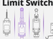
- Everything You Need To Know About Limit Switch - May 21, 2025
- Everthing You Should Know About Rheostat - May 20, 2025
- Everything You Need To Know About Reversing Contactor - May 19, 2025