NAND Flash is a non-volatile storage technology that retains data without power. It dominates modern storage solutions due to its high density, cost-effectiveness, and scalability. Key applications include Solid-State Drives (SSDs), USB drives, memory cards (SD, microSD), and embedded systems in smartphones, IoT devices, and industrial equipment.
Table of Contents
Toggle2. Historical Evolution
- 1984: Dr. Fujio Masuoka of Toshiba invents NAND Flash, building on earlier NOR Flash technology.
- Late 1980s–1990s: Early adoption in portable devices. NOR Flash is used for code storage, while NAND targets data storage due to higher density.
- 2000s: NAND becomes mainstream with digital cameras, MP3 players, and USB drives.
- 2013: Samsung introduces 3D NAND (V-NAND), stacking cells vertically to overcome planar scaling limits.
- 2020s: Quad-Level Cell (QLC) and 3D NAND advancements enable multi-terabyte SSDs.
3. Architecture and Operation
3.1 Basic Structure
- Floating-Gate Transistor: Stores charge in a conductive layer insulated by oxide. Charge presence alters the transistor’s threshold voltage, encoding data.
- Charge Trap Flash (CTF): Newer variant using insulating layer traps instead of conductive floating gates, improving scalability.
3.2 Array Organization
- Pages: Smallest readable unit (4–16 KB).
- Blocks: Smallest erasable unit (128–256 pages, ~256 KB–4 MB).
- Planes/Die: Multiple blocks grouped for parallel operations.
3.3 Read/Write/Erase Mechanics
- Programming: Electrons tunnel into the floating gate via Fowler-Nordheim tunneling.
- Erasing: Block-level removal of electrons using a high voltage.
- Read: Threshold voltage detected to determine bit value.
4. Types of NAND Flash
4.1 Cell Technology
- SLC (Single-Level Cell): 1 bit/cell. Highest endurance (50k–100k P/E cycles), fast, expensive.
- MLC (Multi-Level Cell): 2 bits/cell. Moderate endurance (~3k cycles). Common in consumer SSDs.
- TLC (Triple-Level Cell): 3 bits/cell. Lower endurance (~1k cycles). Dominates cost-sensitive markets.
- QLC (Quad-Level Cell): 4 bits/cell. Lowest endurance (100–1k cycles). Used for high-capacity, read-centric storage.
4.2 3D NAND
- Structure: Cells stacked vertically in layers (64–200+ layers). Increases density without shrinking transistors.
- Advantages: Better endurance, lower power, and higher capacities vs. planar (2D) NAND.
5. Key Applications
- Consumer Electronics: Smartphones (UFS/eMMC), laptops (SSDs), gaming consoles.
- Enterprise Storage: Data centers use NVMe SSDs for low latency/high throughput.
- Automotive: Infotainment, ADAS, and firmware storage with industrial-grade NAND.
- IoT: Low-power, high-density storage for edge devices.
6. Advantages and Challenges
6.1 Advantages
- High Density: Cost per GB decreases with multi-bit cells and 3D stacking.
- Speed: Faster read/write vs. HDDs.
- Durability: No moving parts; resistant to shock/vibration.
6.2 Challenges
- Endurance: Limited write cycles (mitigated by wear leveling, over-provisioning).
- Data Retention: Longer retention at lower temperatures. QLC may retain data for months (vs. years for SLC).
- Error Management: Requires ECC (BCH/LDPC) and RAID-like techniques.
- Read Disturb/Write Amplification: Addressed via controller algorithms.
7. Market Trends and Leaders
- Market Size: $67 billion (2023), growing at ~7% CAGR (2023–2030).
- Key Players: Samsung, Kioxia, Micron, SK Hynix, Western Digital.
- Drivers: Cloud computing, AI, and 5G fueling demand for high-capacity storage.
8. Future Developments
- PLC (Penta-Level Cell): 5 bits/cell. Experimental, with significant endurance trade-offs.
- Advanced 3D NAND: 200+ layers, hybrid bonding (e.g., Xtacking by YMTC).
- Emerging Technologies: MRAM, ReRAM, and PCM may complement NAND but face scalability/cost hurdles.
9. Technical Considerations
- Interfaces: ONFI and Toggle Mode for NAND communication; NVMe/SATA for host interfaces.
- Controllers: Manage ECC, wear leveling, garbage collection, and bad blocks.
- Security: Hardware encryption (e.g., TCG Opal) and secure erase features.
10. Environmental and Industry Impact
- Sustainability: High energy use in fabrication; recycling challenges due to toxic materials.
- Innovation: Transition to 3D NAND reduces reliance on planar scaling, extending Moore’s Law.
11. Conclusion
NAND Flash remains the cornerstone of modern storage, balancing cost, performance, and scalability. While challenges like endurance persist, advancements in 3D stacking and error correction continue to drive its evolution. As emerging technologies mature, NAND will likely coexist with newer memories, ensuring its relevance in the data-driven future.
Further Reading:
- Samsung’s 3D NAND Whitepapers
- IEEE Journals on Non-Volatile Memory
- TechInsights Reports on Flash Memory Trends
This guide provides a foundation for understanding NAND Flash ICs, from basic principles to cutting-edge innovations.

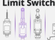
- Everything You Need To Know About Limit Switch - May 21, 2025
- Everthing You Should Know About Rheostat - May 20, 2025
- Everything You Need To Know About Reversing Contactor - May 19, 2025